QuestenaPractice that shows what to review next
Question 368

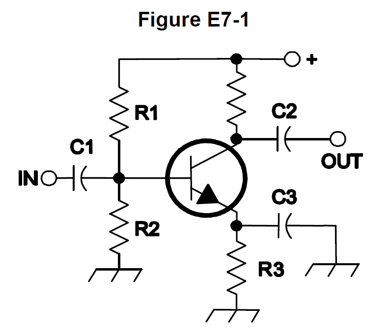
In Figure E7-1, what is the purpose of R1 and R2?

Schematic of a transistor stage with resistors R1, R2, R3, capacitors C1, C2, C3, an input terminal, and an output terminal.
  1. Load resistors
  2. Voltage divider biasCorrect answer
  3. Self bias
  4. Feedback

Explanation

In Figure E7-1, R1 runs from the positive supply to the base and R2 from that same base node to ground, so the two together form a divider that sets the DC base voltage. The collector resistor is the load and R3 in the emitter lead is a separate bias element.
Continue with this test

Start practice
Question 368: In Figure E7-1, what is the purpose of R1 and R2? · FCC Amateur Extra Class (Element 4) · Questena