QuestenaPractice that shows what to review next
Question 369

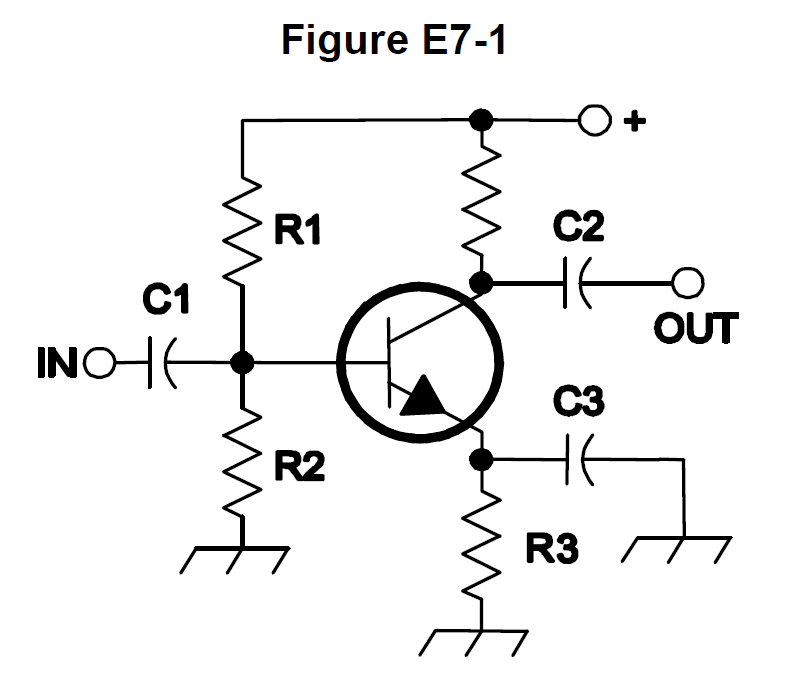
In Figure E7-1, what is the purpose of R3?

Schematic of a transistor stage with resistors R1, R2, R3, capacitors C1, C2, C3, an input terminal, and an output terminal.
  1. Fixed bias
  2. Emitter bypass
  3. Output load resistor
  4. Self biasCorrect answer

Explanation

In Figure E7-1, R3 sits in the emitter lead, so the transistor's own emitter current develops a voltage across it that raises the emitter above ground and reduces the net base-emitter forward voltage. That is self bias, and it stabilizes the operating point against temperature and device spread. Emitter bypassing is done by C3, not by R3.
Continue with this test

Start practice
Question 369: In Figure E7-1, what is the purpose of R3? · FCC Amateur Extra Class (Element 4) · Questena